Circuit Fabrication
Circuits assembled using Breadboards are very flimsy and the wires and components come out very easily. This makes them impractical for real use.
If you want to convert your circuit design into a sturdy assembly, good enough to stand with real-world conditions of power variations, heat, dust, and rough handling, or if you want to create multiple copies of the physical circuit then you need to do what is known as fabricate a circuit on a PCB.
Printed Ciruit Boards (PCBs)
Designing a PCB is a reasonably complex task and we will not be covering it in our projects. If you have a PCB design, there are several online services that fabricating the PCB for you.
A printed circuit board (PCB) mechanically supports and electrically connects electronic and electrical components using conductive tracks, pads, and other features etched from one or more sheet layers of copper laminated onto between sheet layers of a non-conductive substrate. Components are generally soldered onto the PCB to both electrically connect and mechanically fasten them to it. Printed circuit boards are used for electronic circuits in all electronic products.
A basic PCB consists of a flat sheet of insulating material and a layer of copper foil laminated to the substrate. Chemical etching divides the copper into separate conducting lines called tracks or circuit traces, pads for connections, vias to pass connections between layers of copper, and features such as solid conductive areas for electromagnetic shielding or other purposes.
The tracks function as wires fixed in place and are insulated by air and the board substrate material. The surface of a PCB may have a coating that protects the copper from corrosion and reduces the chances of solder shorts between traces or undesired electrical contact with stray bare wires. For its function in helping to prevent solder shorts, the coating is called solder resist or solder mask. "Through-hole" components are mounted by their wire leads passing through the board and soldered to traces on the other side. "Surface mount" components are attached by their leads to copper traces on the same side of the board. A board may use both methods for mounting components. Surface mounting is used for transistors, diodes, IC chips, resistors, and capacitors. Through-hole mounting may be used for some large components such as electrolytic capacitors and connectors.
The pattern to be etched into each copper layer of a PCB is called the "artwork". The etching is often done using a photoresist, which is coated onto the PCB, then exposed to light projected in the pattern of the artwork. The resist material protects the copper from dissolution into the etching solution. After that, the etched board is cleaned. A PCB design can be mass-reproduced similarly photographs can be mass-duplicated from film negatives using a photographic printer.
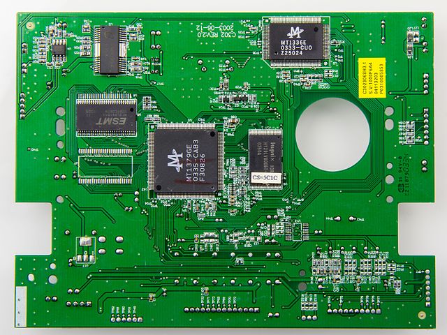
An example of a PCB is shown below. You can see the lines running like train tracks ending at holes where components leads are inserted and soldered. A PCB also has PINs and other text printed on it for instruction or branding purposes.